
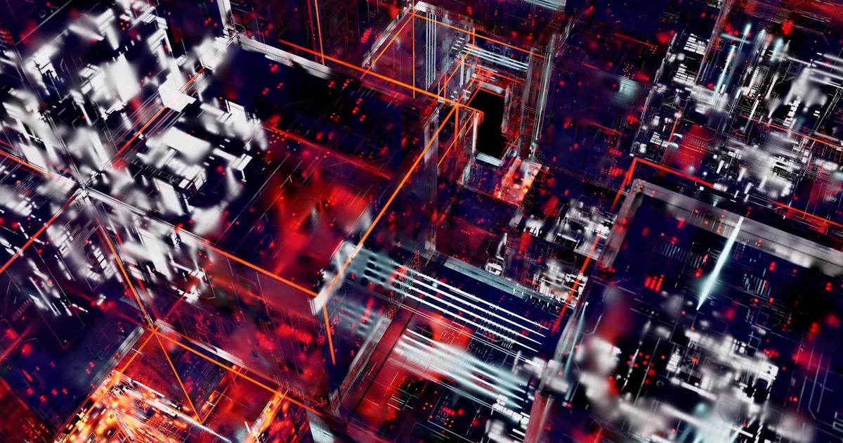
The AI Hardware Revolution: Redefining Intelligence on Silicon
The relentless pursuit of artificial intelligence has propelled us into an era where software innovations are often limited by the underlying hardware. For decades, the Von Neumann architecture, which separates processing from memory, served as the bedrock of computing. However, as AI models grow exponentially in size and complexity, demanding colossal computational power and vast amounts of data movement, this traditional paradigm is showing its cracks. The 'memory wall' – the bottleneck created by the constant shuttling of data between CPU/GPU and external memory – has become the primary impediment to further advancements in AI performance and energy efficiency. The future of AI, therefore, hinges critically on a radical reimagining of its foundational hardware: the AI chip. We stand on the precipice of a new computational era, one defined by specialized, domain-specific architectures designed from the ground up to accelerate intelligence.
The Limitations of Von Neumann and the Rise of AI-Specific Designs
Traditional general-purpose CPUs and even early GPUs, while powerful, were not inherently designed for the unique demands of modern AI workloads, particularly deep learning. Deep learning models thrive on massive parallelism, numerous matrix multiplications, and frequent accumulation operations – tasks that general-purpose architectures can perform, but not with optimal efficiency. The Von Neumann bottleneck manifests as substantial energy expenditure and latency as data constantly moves across the processor-memory divide. This fundamental limitation has spurred a global race to develop AI-specific chips, often termed ASICs (Application-Specific Integrated Circuits) or custom accelerators, meticulously engineered to overcome these challenges. These specialized designs aim to bring computation closer to memory, optimize for AI's characteristic operations, and achieve unprecedented levels of parallel processing, thereby drastically improving performance per watt and reducing the overall energy footprint of AI systems. The shift isn't just about faster clock speeds; it's about fundamentally altering how computation is performed for intelligent tasks.
Beyond Traditional Silicon: Emerging AI Chip Architectures
The next generation of AI chips will move far beyond simple optimization of existing paradigms. They will embrace fundamentally new principles of computation, drawing inspiration from biology, physics, and novel material science. This section explores some of the most promising and disruptive architectural innovations poised to redefine AI hardware.
Neuromorphic Computing: Brain-Inspired Hardware for Ultimate Efficiency
One of the most compelling frontiers in AI chip design is neuromorphic computing. Inspired by the highly efficient, parallel, and event-driven processing of the human brain, neuromorphic chips aim to integrate memory and processing within the same computational units. Unlike traditional synchronous systems, these chips operate asynchronously, processing information only when an 'event' (like a data spike) occurs, much like biological neurons.
- Spiking Neural Networks (SNNs): At the heart of neuromorphic computing are SNNs, which mimic the communication of biological neurons via discrete 'spikes' rather than continuous values. This event-driven approach leads to sparse activation and significantly lower power consumption, especially for tasks involving continuous sensory data processing.
- In-Memory Processing: By co-locating memory and processing units, neuromorphic architectures inherently address the memory wall. This tight coupling allows for vast parallelism and reduces the energy spent on data movement, a major bottleneck in conventional systems.
- Examples: Projects like IBM's TrueNorth and Intel's Loihi are pioneering this space, demonstrating remarkable energy efficiency for specific tasks like pattern recognition, sensory data analysis, and real-time learning at the edge. Their asynchronous nature makes them particularly well-suited for always-on, low-power applications where real-time responsiveness is paramount, opening doors for pervasive AI in embedded systems and IoT devices that operate with stringent power budgets.
Neuromorphic systems promise not just faster AI, but fundamentally more efficient and adaptable AI, capable of learning and adapting with minimal power, potentially unlocking true autonomous intelligence at the edge. They represent a significant paradigm shift from purely numerical processing to a more qualitative, event-driven understanding of information.
In-Memory Computing (IMC) / Processing-in-Memory (PIM): Bridging the Memory-Processor Gap
The concept of bringing computation closer to memory isn't exclusive to neuromorphic designs; it's a broader category known as In-Memory Computing (IMC) or Processing-in-Memory (PIM). This approach directly tackles the Von Neumann bottleneck by performing computations within or very close to the memory modules themselves, drastically reducing data transfer overhead.
- Reducing Data Movement: The core idea is to minimize the energy-intensive and time-consuming process of shuttling data between separate processing units (CPUs/GPUs) and memory (DRAM). By performing operations directly in or near the memory, PIM chips can achieve significant power savings and latency reductions, especially for data-intensive AI tasks.
- Types of PIM:
- Near-memory processing: Logic units are placed very close to memory arrays, often on the same chip or package, allowing for high-bandwidth, low-latency communication.
- In-memory logic: Actual computational operations are performed *within* the memory cells themselves, often by leveraging the physical properties of memory technologies like non-volatile memories (e.g., ReRAM, PCM). For example, a resistive RAM (ReRAM) crossbar array can naturally perform vector-matrix multiplications – the cornerstone of neural networks – by applying voltages to rows and reading currents from columns, effectively doing analog computation in situ.
- Impact on AI: PIM is particularly potent for deep learning, where repeated matrix multiplications and accumulations are dominant operations. By performing these operations where the weights and activations reside, PIM architectures can deliver substantial improvements in throughput and energy efficiency, making larger and more complex models feasible at lower power budgets. Companies like Samsung and various startups are actively exploring and implementing PIM solutions for commercial AI accelerators.
Analog AI Chips: Speed and Power for Precision-Tolerant Tasks
While most digital computers rely on binary '0s' and '1s', analog computing leverages continuous physical properties (like voltage or current) to represent data and perform operations. Analog AI chips can perform computations, particularly matrix-vector multiplications, extremely efficiently.
- Efficiency and Speed: In deep learning, many operations, like weighting inputs, are essentially analog by nature. Performing these directly in the analog domain avoids the energy overhead and latency associated with digital-to-analog and analog-to-digital conversions. This can lead to significant gains in speed and power efficiency, especially for inference tasks where a certain degree of imprecision is tolerable.
- In-Memory Analog Computing: Often, analog AI chips implement in-memory computing principles, using resistive memory elements (like ReRAM or phase-change memory) as synapses whose conductance can be programmed to represent network weights. Applying input voltages across these resistors results in currents that are proportional to the product of voltage and conductance, effectively performing analog multiplication and summation in parallel.
- Challenges: The main challenges include precision loss, noise susceptibility, and difficulty in programming and recalibrating the analog components. However, for inference tasks where energy consumption and latency are paramount, and where AI models are robust to minor numerical variations, analog AI offers a compelling pathway to ultra-efficient acceleration. Recent advancements in materials and calibration techniques are rapidly overcoming these limitations.
Optical Computing: Harnessing the Speed of Light
Imagine computation not limited by the flow of electrons, but by the speed of light itself. Optical computing leverages photons instead of electrons to perform computations, offering tantalizing prospects for unparalleled speed and energy efficiency.
- Advantages:
- Speed: Light travels much faster than electrons through silicon, theoretically allowing for much higher clock speeds and lower latency.
- Parallelism: Different wavelengths of light can travel through the same medium without interfering, enabling massive parallel processing – a dream for highly parallel AI workloads.
- Low Power Dissipation: Photons do not generate heat in the same way electrons do when moving through resistance, promising drastically reduced power consumption for certain operations.
- Interconnections: Optical interconnects can overcome the bottleneck of electrical wiring on chips, allowing for higher bandwidth data transfer within and between chips.
- AI Applications: Optical computing is particularly well-suited for linear algebra operations, such as matrix multiplications, which are the fundamental building blocks of neural networks. Optical components like interferometers can be arranged to perform these operations at the speed of light.
- Challenges: Miniaturization, integration with existing electronic systems, and efficient optical-to-electrical conversion remain significant engineering hurdles. Despite these challenges, companies and research institutions are making rapid progress, demonstrating fully optical neural network accelerators that can perform inference at incredible speeds with very low power. The synergy of optical computing with deep learning could unlock AI capabilities currently unimaginable with purely electronic systems.
Materials and Integration: The Foundation for Next-Gen Chips
Beyond architectural innovations, the very fabric of AI chips is undergoing a revolution driven by advanced materials science and sophisticated integration techniques. These foundational advancements are critical enablers for the novel computing paradigms discussed above.
3D Stacking and Heterogeneous Integration: Building Up, Not Just Out
As miniaturization in 2D approaches physical limits, chip designers are increasingly looking upwards. 3D stacking involves vertically integrating multiple layers of components (processors, memory, sensors) within a single package.
- Benefits:
- Reduced Interconnect Lengths: Shorter vertical connections (via through-silicon vias or TSVs) drastically reduce latency and power consumption compared to long horizontal wires.
- Higher Bandwidth: More connections packed into a smaller footprint enable much higher data transfer rates between stacked components, directly addressing the memory wall.
- Increased Density: More functionality can be packed into a smaller physical volume, crucial for edge AI devices.
- Heterogeneous Integration: This concept takes 3D stacking a step further by integrating different types of components – not just multiple layers of the same type – onto a single package. This could mean integrating a custom AI accelerator, high-bandwidth memory (HBM), and even optical components side-by-side or stacked vertically. This allows for the 'best-of-breed' approach, where specialized chips (e.g., for vision, language, or general computation) are optimized individually and then seamlessly integrated, leading to highly efficient, domain-specific AI systems. This modular approach offers flexibility and optimizes resources for varied AI workloads.
Novel Materials: Beyond CMOS and Silicon
For decades, silicon and CMOS (Complementary Metal-Oxide-Semiconductor) technology have been the bedrock of microelectronics. While silicon remains dominant, the demands of future AI chips are pushing the boundaries towards new materials with superior properties.
- Beyond Silicon: Materials like graphene, molybdenum disulfide (MoS2), and other 2D materials offer extraordinary electronic and thermal properties. Their atomic thinness could enable further miniaturization, higher switching speeds, and potentially novel device architectures.
- Resistive Memory (RRAM/ReRAM, PCM): These non-volatile memory technologies are crucial for in-memory and analog AI computing. Their ability to change and retain resistance based on applied voltage makes them ideal candidates for artificial synapses in neuromorphic and analog accelerators. They offer high density, low power operation, and endurance far beyond traditional DRAM.
- Spintronics: This emerging field exploits the 'spin' of electrons in addition to their charge. Spintronic devices could offer non-volatility, lower power consumption, and new computational paradigms, potentially leading to more energy-efficient and faster memory and logic components for AI.
- Superconductors: While requiring extremely low temperatures, superconducting circuits offer zero electrical resistance, enabling ultra-fast, energy-efficient computation. Advances in high-temperature superconductors could one day make this a more practical option for specialized, high-performance AI supercomputers.
These advanced materials, coupled with sophisticated integration techniques, are not merely incremental improvements; they are foundational shifts that enable entirely new modes of computation and packaging for the AI chips of tomorrow.
Quantum Computing's Long-Term Role: A Glimpse into the Future
While not immediately a direct 'chip architecture' for today's AI, quantum computing holds immense long-term potential for specific, computationally intensive AI tasks. Algorithms like quantum machine learning could offer exponential speedups for certain optimization problems, pattern recognition, and data analysis that are intractable for even the most powerful classical supercomputers. While general-purpose quantum AI remains far off, its specialized applications might one day complement or accelerate classical AI chip architectures, particularly for training complex models or discovering new algorithms. Its impact, while not direct on current AI chip design, is a crucial consideration for the ultimate trajectory of AI hardware.
Software-Hardware Co-design: A Necessary Symbiosis for Optimal AI
In the past, hardware and software development often proceeded independently. However, for future AI chips, a tightly coupled, symbiotic relationship – known as software-hardware co-design – is becoming absolutely essential. Without it, even the most innovative chip architecture will fail to reach its full potential.
Optimizing for AI Workloads: A Holistic Approach
AI models are incredibly diverse, from small, efficient models for edge devices to massive, multi-modal models demanding petabytes of data. A 'one-size-fits-all' chip is increasingly inefficient. Software-hardware co-design entails:
- Algorithm-Specific Architectures: Designing hardware accelerators that are explicitly optimized for the mathematical operations and data flow patterns of specific AI algorithms (e.g., CNNs for vision, Transformers for language, reinforcement learning). This means understanding the compute and memory access patterns of an algorithm and tailoring the hardware to perform those operations with maximum efficiency.
- Compiler and Runtime Integration: Developing compilers and runtime systems that can intelligently map AI models onto the heterogeneous and novel hardware architectures. This involves optimizing data placement, parallelism, and operation scheduling to extract peak performance from specialized units.
- Domain-Specific Languages (DSLs): Creating new programming languages or extensions that allow AI developers to express their models in a way that directly translates to efficient execution on custom hardware, abstracting away the underlying architectural complexities.
- Quantization and Sparsity-Aware Design: Integrating hardware support for techniques like model quantization (reducing numerical precision) and sparsity (exploiting inactive neurons) directly into the chip architecture. This can dramatically reduce memory footprint and computational requirements, leading to more efficient AI at inference.
Reconfigurable Architectures: Adaptability in a Dynamic AI Landscape
The AI landscape is constantly evolving, with new models and algorithms emerging regularly. Fixed-function ASICs, while highly efficient for specific tasks, can quickly become obsolete. This calls for reconfigurable architectures.
- FPGAs (Field-Programmable Gate Arrays): FPGAs offer a balance between flexibility and performance. They consist of programmable logic blocks and interconnects that can be configured and reconfigured to implement custom logic circuits. This allows for adapting the hardware to different AI models or evolving algorithms post-deployment. While generally less performant than ASICs for a given task, their adaptability is a significant advantage in rapidly changing AI environments.
- Coarse-Grained Reconfigurable Arrays (CGRAs): CGRAs provide a higher level of reconfigurability than FPGAs, often featuring an array of processing elements that can be connected in various ways to form domain-specific accelerators. They offer better performance and energy efficiency than FPGAs for typical AI workloads while retaining significant programmability.
- Modular and Adaptable Designs: Future AI chips will likely feature a blend of fixed-function accelerators for common AI primitives (e.g., matrix multiplication units) and reconfigurable units for newer algorithms or specialized workloads. This hybrid approach ensures both high efficiency for standard tasks and the flexibility to adapt to future innovations.
The future of AI hardware isn't just about building faster chips; it's about building smarter, more adaptable chips that are intimately designed with the software they run, allowing for a harmonious and highly optimized AI ecosystem.
Challenges and the Road Ahead: Navigating the Future of AI Chips
The journey towards these revolutionary AI chip architectures is fraught with significant challenges, spanning engineering, economic, and systemic hurdles. Overcoming these will be crucial for realizing the full potential of next-generation AI.
Manufacturing Complexity and Cost: The Fabrication Barrier
- Novel Materials Integration: Working with new materials like 2D materials, spintronics, or advanced resistive memories introduces immense complexity into fabrication processes. Integrating these with existing silicon technologies requires new manufacturing techniques, specialized equipment, and stringent quality control, which can be prohibitively expensive.
- 3D Stacking Challenges: Achieving high-yield manufacturing for 3D integrated circuits, especially with heterogeneous components, demands extremely precise alignment, thermal management solutions for stacked layers, and reliable through-silicon vias (TSVs). Each additional layer and each new material adds to the manufacturing difficulty and cost.
- Economic Viability: The non-recurring engineering (NRE) costs for designing and fabricating advanced semiconductor chips are already skyrocketing. For highly specialized AI ASICs, the market needs to be large enough to justify these enormous upfront investments. This often necessitates large-volume production or widespread adoption of specific architectural standards, which is a chicken-and-egg problem.
Programming Models and Toolchains: The Software Bottleneck
- New Paradigms, New Software: Architectures like neuromorphic and optical computing operate on fundamentally different principles than traditional digital systems. This necessitates entirely new programming models, languages, and development toolchains that can effectively translate high-level AI algorithms into the unique operations of these chips. Existing software ecosystems are ill-equipped to handle these novel paradigms.
- Abstraction and Usability: For these new chips to gain widespread adoption, developers need easy-to-use frameworks and libraries that abstract away the low-level hardware intricacies. Creating efficient compilers that can map complex AI graphs onto highly heterogeneous and reconfigurable hardware is a monumental task.
- Debugging and Verification: Debugging errors in deeply integrated, potentially analog, or asynchronous systems is far more challenging than in traditional digital circuits. Robust verification methodologies are paramount to ensure the correctness and reliability of these complex systems.
Economic Viability and Ecosystem Development: Building a New Industry
- Standardization: The proliferation of diverse AI chip architectures creates a fragmentation problem. Without some degree of standardization or interoperability, developing and deploying AI models across different hardware platforms becomes incredibly cumbersome. This requires industry-wide collaboration and potentially new open standards for hardware interfaces and software APIs.
- Market Adoption: Convincing the industry to switch from established, albeit less efficient, hardware platforms to new, unproven technologies requires compelling performance gains, robust reliability, and a clear path to return on investment. The cost of transitioning entire infrastructure to new AI hardware can be a significant barrier.
- Talent Gap: Designing, fabricating, and programming these next-generation AI chips demands a highly specialized skillset at the intersection of computer architecture, materials science, electrical engineering, and AI/machine learning. There is a growing talent gap in these interdisciplinary areas.
The Impact on AI's Future: Unlocking Unprecedented Capabilities
Despite these challenges, the impetus for developing future AI chip architectures is undeniable due to the transformative impact they promise. These advancements will not merely make existing AI faster; they will fundamentally alter what AI can achieve.
Democratizing Advanced AI: Pervasive and Accessible Intelligence
- Edge AI Explosion: Highly efficient AI chips will enable sophisticated AI models to run directly on edge devices – smartphones, drones, autonomous vehicles, smart sensors – without constant reliance on cloud connectivity. This will lead to real-time responsiveness, enhanced privacy, reduced latency, and lower operational costs. Imagine medical diagnostics on a wearable device or real-time environmental monitoring by tiny, self-powered sensors.
'The decentralization of advanced AI capabilities from centralized data centers to ubiquitous edge devices, powered by these efficient new chips, promises to democratize intelligence on an unprecedented scale,' notes Dr. Anya Sharma, a leading expert in edge AI computing. 'This shift will profoundly impact accessibility, privacy, and the sheer pervasiveness of smart systems in our daily lives.'
- Lowering the Cost of AI: By drastically reducing the power consumption and physical footprint required for AI computation, these new chips will make advanced AI more accessible and affordable for a broader range of applications and organizations, moving AI beyond the exclusive domain of tech giants.
- Sustainable AI: The current energy footprint of large AI models is staggering. Future chips, with their emphasis on efficiency, are crucial for making AI development and deployment more environmentally sustainable, aligning with global efforts to reduce carbon emissions.
New Frontiers in Application: Unleashing Unimagined Possibilities
- Hyper-Personalized AI: With greater on-device intelligence and efficiency, AI systems can become deeply personalized, adapting to individual users' preferences, contexts, and learning styles in real-time, from personalized education to proactive health monitoring.
- Complex Scientific Discovery: Accelerating scientific simulations, drug discovery, materials science research, and climate modeling will unlock breakthroughs previously limited by computational power. Large-scale AI models running on these chips could analyze vast datasets and identify patterns intractable for human researchers.
- Truly Autonomous Systems: The combination of real-time processing, low power, and robust performance from future AI chips is essential for truly autonomous systems – from self-driving cars navigating complex urban environments to intelligent robots performing delicate surgical procedures or exploring distant planets. These systems demand millisecond responsiveness and absolute reliability, something current general-purpose hardware struggles to deliver consistently.
- Multi-Modal AI and AGI: The ability to process and fuse information from multiple modalities (vision, sound, text, touch) efficiently, combined with the computational horsepower to train larger, more generalizable models, brings us closer to Artificial General Intelligence (AGI) – AI that can understand, learn, and apply intelligence across a broad range of tasks, much like a human. Future chips are a foundational requirement for such advanced cognitive architectures.
Conclusion: A Future Forged in Silicon and Light
The trajectory of AI is inextricably linked to the evolution of its underlying hardware. The era of general-purpose computing struggling to keep pace with AI's voracious demands is drawing to a close. We are witnessing the dawn of a new age, where specialized, brain-inspired, optical, and in-memory computing architectures will redefine what's possible. From neuromorphic chips mimicking the brain's energy efficiency to optical processors harnessing the speed of light, and from sophisticated 3D integration to novel materials, the innovation pipeline for AI chips is richer and more diverse than ever before.
While significant technical and economic challenges lie ahead, the promise of more efficient, powerful, and pervasive AI is too compelling to ignore. The symbiotic relationship between software and hardware will deepen, leading to co-designed systems that are not just faster, but fundamentally smarter and more adaptable. These future AI chip architectures will not merely accelerate existing applications; they will unlock entirely new frontiers of intelligence, driving breakthroughs across every sector of human endeavor, ushering in an unprecedented era of intelligent systems that are both powerful and inherently sustainable. The future of AI is being etched, one atomic layer at a time, into these revolutionary new forms of silicon and beyond. It's a future where intelligence is not just processed, but inherently architected into the very fabric of computation.